Embedded Die Packaging Technology Market Statistics, 2031
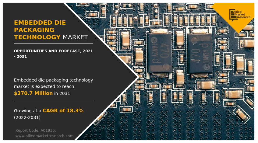
The global embedded die packaging technology market was valued at $69.2 million in 2021 and is projected to reach $370.7 million by 2031, growing at a CAGR of 18.3% from 2022 to 2031. Embedded die packaging technology is a native 3D-compatible packaging solution, offering nearly 70% size reduction in in package (SiP) solution. The advantages of this technology include miniaturization, improved electrical & thermal performance, heterogeneous integration, prospects for cost reduction, and efficient logistics for OEM. In addition, it offers flexible system integration, fast turnaround for custom design, high robustness, and enhanced reliability of the package.
The growth of global embedded die packaging technology is mainly driven by the increasing demand for 5G network technology and consumer electronics. Numerous consumer electronic devices, such as smartphones, laptops, tablets, and portable gaming consoles, incorporate several embedded chips to provide a better user interface and enhanced overall performance. In smartphones, wearable devices, and other consumer electronic appliances, these chips are used primarily in DC-DC converters, power electronic circuitry, and camera circuits.

Moreover, due to the incorporation of 5G into their architecture, embedded devices used in smart video surveillance systems of automobiles give rapid response times. There is also a critical need for circuit miniaturization in microelectronic devices. Embedded die packaging is a promising technology for emerging microwave applications, owing to its excellent electrical performance at high frequencies. With the reduction in size of electronic devices for ease of access for users, the demand for compact electronic circuitry is on the rise. This demand is met by embedded die packaging technology, which offers advantages such as increased functionality & efficiency of the electronic circuit; reduced size, signal inductance & power inductance; improved reliability; and higher signal density. Compact size is one of the several advantages offered by embedded die packaging technology. This technology offers 70% less chip area as compared to SiP technology. Moreover, embedded die packaging technology has several advantages, such as enhanced chip quality, superior reliability, and better security. Unlike other technologies, in embedded die packaging, the die is embedded and thus consumes no area on the chip.
Embedded die packaging technology is a costly technology; therefore, it is a potential restraint and will hamper the growth of the market. With the rising cost of packaging technology and the presence of fewer companies in this business, there are fewer competitors, making this market a spot for exploitation. On the other hand, the increasing implementation of the Internet of Things (IoT) is an opportunity for the market during the forecast period. The Internet of Things (IoT) is a technology that interconnects daily-use objects and allows them to exchange data through a wireless medium. This is facilitated with the help of miniature electronic circuits attached inside these devices to enable the sharing of data and control of the flow of information between them. These electronic circuits use microcontrollers, microprocessors, and other small components. The basic requirement of power electronic circuitry used in these devices is small size, low power consumption, less heat dissipation, and a smaller form factor. These needs are fulfilled with the use of chips fabricated with embedded die packaging technology.
Segmentation Overview:
The embedded die packaging technology market is segmented into Platform and Industry Vertical.
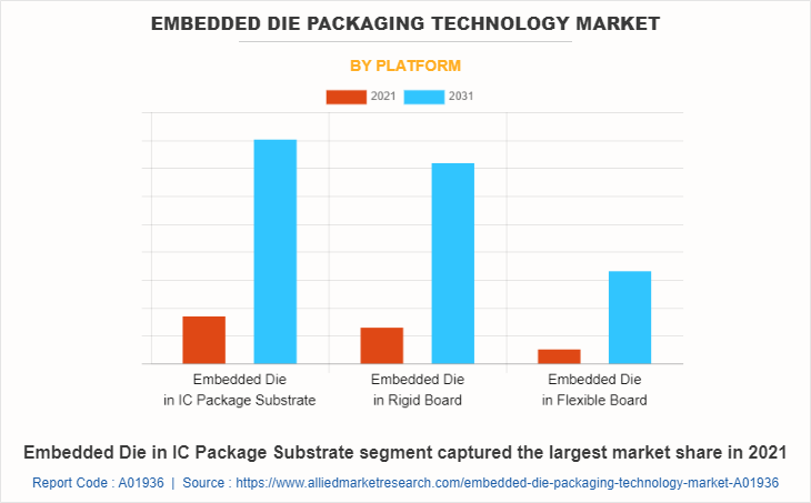
Based on the platform, it is segmented into embedded die in IC package substrate, embedded die in rigid board, and embedded die in flexible board. According to the embedded die packaging technology market analysis, the embedded die in IC package substrate segment was the highest contributor to the market in 2021, whereas the embedded die in flexible board is expected to expand at a faster rate during the forecast period.

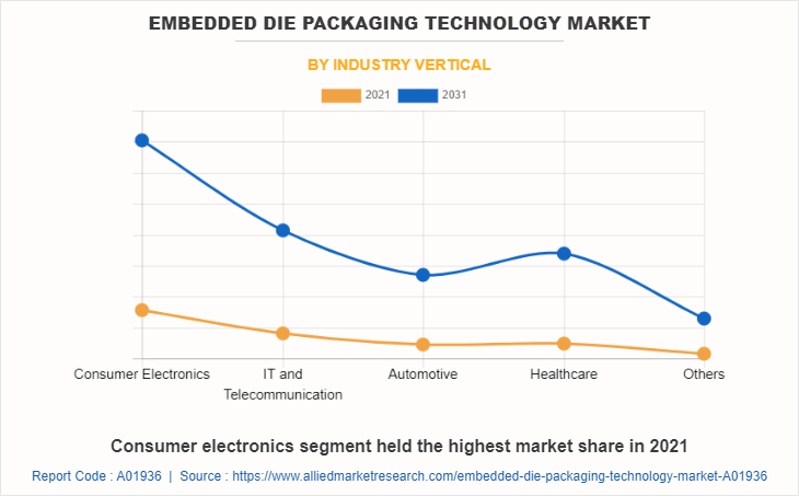
Based on industry vertical, the market is segmented into consumer electronics, IT and telecommunication, automotive, healthcare, and others. The consumer electronics and IT & telecommunication segments collectively accounted for the majority of the embedded die packaging technology market share in 2021. A surge in prime players' initiatives to develop and deploy next-generation portable device solutions globally has led to the growth of the consumer electronics and IT & telecommunication segment, thereby enhancing the embedded die packaging technology market growth. Meanwhile, the other segment is estimated to grow at a faster rate during the forecast period.

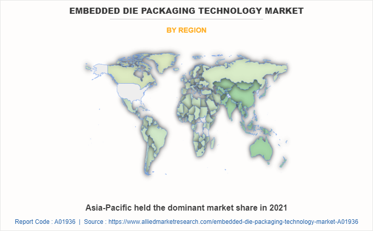
Region-wise, the market is analyzed across North America, Europe, Asia-Pacific, and LAMEA. Asia-Pacific holds a significant share in the global embedded die packaging technology market size, owing to the presence of prime players in this region, and it is also expected to be the fastest-growing region during the forecast period. Further, China holds a dominating position in the Asia-Pacific embedded die packaging technology market forecast owing to rise in investment by prime players and government agencies to develop next generation embedded die packaging technology-based semiconductor solution to improve electrical thermal performance and reliability & mechanical stability, which is expected to lead to the growth of the embedded die packaging technology in this region.

Competition Analysis
Competitive analysis and profiles of the major embedded die packaging technology market players that have been provided in the report include Amkor Technology, Taiwan Semiconductor Manufacturing Company, ASE Group, AT & S, General Electric, Infineon, Fujikura, MicroSemi, TDK-Epcos, and Schweizer. These key players adopt several strategies, such as new product launch, acquisition, partnership, joint venture, and collaboration, to increase their market share in the global embedded die packaging technology market opportunity during the forecast period.
Top Impacting Factors
The growth of the global embedded die packaging technology market is majorly driven by the surge in demand for consumer electronics and 5G network technology, coupled with the impending need for circuit miniaturization in microelectronic devices. Another factor driving its market is the technology’s advantages over other IC packaging technologies, especially its ability to use 70% less chip area in comparison to SiP technology. However, high initial cost acts as a prime restraint on the global embedded die packaging technology market outlook. On the contrary, the rise in trends related to Internet of Things (IoT) solutions is anticipated to provide lucrative opportunities for embedded technology and the embedded die packaging technology industry during the forecast period.
Historical Data and Information
The embedded die packaging technology industry is fairly competitive, owing to the strong presence of existing vendors. Market vendors are expected to gain a competitive advantage over their competitors because they can cater to market demands with a wide range of products. The competitive environment in this market is expected to increase as technological innovations, product extensions, and different strategies are adopted by key vendors.
Key Developments/Strategies
Taiwan Semiconductor Manufacturing Company, General Electric, Infineon, Fujikura, and Amkor Technology are among the top companies that hold a prime share in the embedded die packaging technology market. Top market players have adopted various strategies, such as product launches, contracts, and others, to expand their foothold in the embedded die packaging technology market.
- In November 2021, Amkor announced the business expansion of advanced packaging technology capacity with a new factory setup in Bac Ninh, Vietnam. This was expected to provide a long-term investment in geographical diversification and factory capacity expansion, supporting Amkor's commitment to reliable supply chain solutions for its customers.
- In October 2022, Amkor Technology, Inc. introduced 5G RF module design, characterization, and packaging technology. With the introduction of 5G, cellular frequency bands have increased considerably, requiring innovative solutions for the packaging of RF front-end modules for smartphones and other 5 G-enabled devices.
- In February 2021, Siemens and ASE, in collaboration for package design, developed and introduced enablement technologies for next-generation high-density advanced package designs. The new high-density advanced packaging (HDAP) enablement solutions stem from ASE's participation in the Siemens OSAT Alliance, a program designed to drive faster adoption of new HDAP technologies like 2.5D and 3D ICs and fan-out wafer-level packaging (FOWLP) for next-generation IC designs.
- In May 2022, Fujikura, Ltd. announced it is collaborating with GlobalFoundries (GF) in enabling the commercial availability of Future Access, the industry's most integrated 28GHz 5G mm Wave module, for both mobile and fixed wireless infrastructure markets.
- In November 2021, Schweizer Electronic founded its own sales company in the USA, based in Wilmington, Delaware. In addition to its headquarters in Schramberg, Germany, as well as its new, state-of-the-art high-tech production facility in Jintan, China, the company gained greater access to the American market with a focus on the U.S., Canada, and Mexico. SCHWEIZER will address the target markets of automotive, aviation, and industry in particular.
Key Benefits for Stakeholders
- This report provides a quantitative analysis of the market segments, current trends, estimations, and dynamics of the embedded die packaging technology market from 2021 to 2031 to identify the prevailing embedded die packaging technology market opportunities.
- The market research is offered along with information related to key drivers, restraints, and opportunities.
- Porter's five forces analysis highlights the potency of buyers and suppliers to enable stakeholders to make profit-oriented business decisions and strengthen their supplier-buyer network.
- In-depth analysis of the embedded die packaging technology market segmentation helps determine the prevailing market opportunities.
- Major countries in each region are mapped according to their revenue contribution to the global market.
- Market player positioning facilitates benchmarking and provides a clear understanding of the present position of the market players.
- The report includes the analysis of the regional as well as global embedded die packaging technology market trends, key players, market segments, application areas, and market growth strategies.
Embedded Die Packaging Technology Market Report Highlights
| Aspects | Details |
| Market Size By 2031 | USD 370.7 million |
| Growth Rate | CAGR of 18.3% |
| Forecast period | 2021 - 2031 |
| Report Pages | 236 |
| By Platform |
|
| By Industry Vertical |
|
| By Region |
|
| Key Market Players | Amkor Technology Inc., SCHWEIZER ELECTRONIC AG, Infenion Technologies AG, Microsemi, Taiwan Semiconductor Manufacturing Company Limited, AT&S Group, General Electric, TDK Corporation, ASE GROUP, Fujikura |
Analyst Review
Embedded die packaging technology can be explained as the process of positioning or molding the components or ICs that are on an internal layer of an organic circuit board, unit, or chip package, such that it is hidden inside the complete structure, in spite of being connected on the top or bottom. The global embedded die packaging technology market is highly competitive, owing to the strong presence of existing vendors. Embedded die packaging technology vendors, who have access to extensive technical and financial resources, are anticipated to gain a competitive edge over their rivals, as they have the capacity to cater to the market requirements. The competitive environment in this market is expected to further intensify with increase in technological innovations, product extensions, and different strategies adopted by key vendors.
The rise in demand for enhanced printed circuit boards, ICs and Chips solutions across consumer electronics and telecommunication sector globally is driving the need for next generation semiconductor packaging solution to enhance embedded die packaging technology solutions. Moreover, prime economics, such as the U.S., China, Germany, and Japan, plan to develop and deploy next generation embedded die packaging electronics solutions such as portal devices, digital TVs, and more, which is anticipated to provide lucrative opportunities for market growth. North America is the second highest revenue contributor to the global market, after Asia-Pacific. The market growth is attributed to factors such as rise in R&D investment in automotive industry, well-established IT & telecommunication industry, and surge in number of smart homes. The key players in the embedded die packaging technology market are Amkor Technology, Taiwan Semiconductor Manufacturing Company, ASE Group, AT & S, General Electric, Infineon, Fujikura and MicroSemi.
The embedded die packaging technology market was valued at $69.18 million in 2021
Embedded Die in IC Package Substrate is the leading platform of the embedded die packaging technology market
Asia-Pacific is the largest regional market of embedded die packaging technology market
The market embedded die packaging technology market is expected to grow at CAGR of 18.3%
The key players operating in the embedded die packaging technology market are Amkor Technology, Taiwan Semiconductor Manufacturing Company, ASE Group, AT & S, General Electric, Infineon, Fujikura, MicroSemi, TDK-Epcos, and Schweizer.
Loading Table Of Content...
Loading Research Methodology...


