
Silicon EPI Wafer Market Overview:
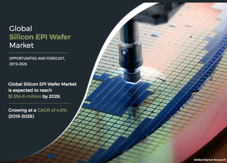
The Global Silicon EPI Wafer Market size was valued at $1.15 billion in 2018, and is projected to reach $1.55 billion by 2026, growing at a CAGR of 4.8% from 2019 to 2026. Silicon EPI wafer is an exotic semiconducting material. It is combined with epitaxial growth that is a deposition of a crystalline layer over a crystalline-based semiconductor substrate, called silicon EPI wafer. These wafers are used as a high purity layer and for the formation of thick dopes. An epitaxial wafer is used for photonics, microelectronics, spintronics, or photovoltaics in various application such as smart phones, LED, gyroscope, laptops, tablets, gaming consoles, and others.
Advancements in silicon EPI wafer deliver highly efficient and reliable electrical interconnect solutions for electronic products. The market holds a great potential in electronics and IT & telecommunication industries. Thus, increased adoption of advance wafer technology in portable electronics is expected to propel the demand for silicon EPI wafer in the future.
The demand for silicon EPI wafers semiconductors has increased in the recent years due to their advantages such as higher efficiency, lightweight, less space consumption, and flexibility in shape as compared to conventional silicon (c-Si). They are widely used in various applications such as solar photovoltaic panels, DRAMs, microprocessors, and wearable technologies.
By Type
Homoepitaxy is projected as one of the most lucrative segments.
The rise in demand for silicon EPI wafer technology in industries such as electronics, IT & telecommunication, and automotive is expected to supplement the silicon EPI wafer market growth. Silicon EPI wafer enables high functionality with least cost when dealing with complex ICs having multiple input/output connections to the outside world. The key factors driving the growth of the global silicon EPI wafer market are technological superiority than conventional silicon, high demand due to increase in usage in emerging applications such as DRAM, flexible OLED displays, and AMOLED displays, rise in demand for higher efficiency and miniaturization, and growth in investment in solar power plants.
By Wafer Size
12 inch is expected to secure leading position during forecast period.
The factors such as increase in demand for epitaxial wafer in consumer electronics, growth in usage of GPS, emerging trends of wafer in automotive industry, and rise in the semiconductor industry boost the growth of the silicon EPI wafer market globally. However, increase in shift from homoepitaxy to heteroepitaxy deposition type that increase the overall cost of wafer manufacturing is expected to hamper the Silicon EPI Wafer Market growth.
By Region
Asia-Pacific region would exhibit the highest CAGR of 5.5% during 2019-2026
SEGMENTATION
The global silicon EPI wafer market is segmented on the basis of type, wafer size, application, industry vertical, and region. By type, the market is bifurcated into Heteroepitaxy and Homoepitaxy. By wafer size, the market is divided into 6-inch, 8-inch, 12-inch, and others. By application, the market is studied across LED, power semiconductor, and MEMS-based devices. By industry vertical, the silicon EPI wafer market is categorized into consumer electronics, automotive, healthcare, industrial, and others. Furthermore, others is subsegmented into telecommunication and lighting. By region, it is analyzed across North America, Europe, Asia-Pacific, and LAMEA along with their prominent countries.
The key players profiled in the silicon EPI wafer industry report include Nichia Corporation, Applied Materials, Sumco Corporation, Epigan, ASM, Global Wafers, Siltronic, Wafer World Inc., Tokyo Electron, and Shin Etsu Chemical Co. Ltd. These key players have adopted strategies, such as product portfolio expansion, mergers & acquisitions, agreements, geographical expansion, and collaborations to enhance their market penetration.
TOP IMPACTING FACTORS
The notable factors positively affecting the silicon EPI wafer market share growth include emerging trends of wafers in an automotive industry and growth in the semiconductor industry. However, increase in the cost of wafer manufacturing hampers the market growth. This factor is expected to slow down the silicon EPI wafer market growth. Moreover, growth of smart lighting and increase in popularity of IoT in wafers offers huge silicon EPI wafer market opportunities in the next six years.
Emerging trends of wafers in automotive industry
Wafers have become an intrinsic part of the production process, as they help increase the efficiency and precision through automation. Wafers are used to keep a track of various parameters such as temperature, pressure, flow, level, and other parameters to control the whole process and ease it through robots. In addition, an increase in production rate in the automotive industry in which the contribution from the autonomous vehicles, electric vehicles, and self-driving trucks is expected to play a vital role. Thus, production of vehicles is anticipated to create a lot of opportunities for the vendors in the silicon epitaxial wafers market.
Increase in cost of wafer manufacturing
Silicon EPI wafer is a semiconductor device fabrication step during which wafer thickness is reduced to allow stacking and high-density packaging of integrated circuits. This is expected to add up to the overall wafer manufacturing cost by making it slightly expensive. This increase in shift from homoepitaxy to heteroepitaxy increase the overall cost of wafer manufacturing, which is expected to hamper the growth of the silicon EPI wafer market up to a certain level. Complexities associated with the design are anticipated to restraint the silicon EPI wafer market growth.
Increase in popularity of IoT in wafers
In the current IT-dominant world, people are moving toward automation-based solution and services. This has led to increased focus on IoT-based devices due to their innovative and advanced applications. IoT is a technology for providing internet or internetworking for almost all applications such as smartphones, microwaves, refrigerators, and buildings. IoT uses electronic software, wafers for connecting all these things to a common network. IoT incorporates several wafers such as epitaxial wafer. The semiconductor industry has witnessed considerable growth over the past few years due to factors such as emergence of IoT, cloud computing, data analytics, and AI. This increase in trends in semiconductor devices and materials creates huge demand for wafers and chips.
Key Benefits for silicon Epi Wafer Market:
- This study includes the analytical depiction of the global silicon EPI wafer market trends along with the current trends and future estimations to determine the imminent investment pockets.
- The silicon EPI wafer market is determined to understand the profitable trends to gain a stronger foothold.
- The report presents information related to key drivers, restraints, and opportunities with a detailed impact on silicon EPI wafer market analysis.
- The current silicon EPI wafer market forecast is quantitatively analyzed from 2018 to 2026 to benchmark the financial competency.
- Porter’s five forces analysis illustrates the potency of the buyers and suppliers in the silicon EPI wafer market.
- The report includes the silicon EPI wafer market share of key vendors and market trends.
Silicon EPI Wafer Market Report Highlights
| Aspects | Details |
| By Type |
|
| By Wafer Size |
|
| By Application |
|
| By Industry Vertical |
|
| By Region |
|
| Key Market Players | SUMCO CORPORATION, WAFER WORLD INC., APPLIED MATERIALS. INC., SILTRONIC, NICHIA CORPORATION, ASM INTERNATIONAL N.V., SHOWA DENKO K.K, SHIN-ETSU CHEMICAL CO., LTD, TOKYO ELECTRON LTD., GLOBAL WAFER |
Analyst Review
Silicon EPI using semiconductor substrate materials and includes ICs, MEMS, and other microelectronic components on a single chip. They have bumps on one side to facilitate connections to circuits. The silicon EPI wafer includes various type of application such as gyroscope, LED, laptops, tablets, gaming consoles, smartphones, flourishing electronics for photonics, microelectronics, spintronics, photovoltaics, and others. The MEMS -based devices application holds the largest share in overall silicon EPI wafer market across the globe. The implementation of LEDs made with EPI wafer in electronic devices drives its growth in the overall silicon EPI wafer market.
Major factors propelling the demand for silicon EPI wafer market are the widely extending applications in rapidly growing technologies such as solar photovoltaic panels, DRAMs, microprocessors, flexible OLED displays, AMOLED displays, and MEMS. Moreover, impending need of circuit miniaturization, high investment by various governments in solar power plants, and technological developments in organic LED displays supplement the growth of the market.
The demand for Silicon EPI Wafer in the commercial sector is expected to increase rapidly during the forecast period. Increasing demand for epitaxial wafer in consumer electronics, growing usage of GPS, emerging trends of wafer in automotive industry, and developing semiconductor industry boosts the growth of the silicon EPI wafer market globally. However, increase in shift from homoepitaxy to heteroepitaxy deposition type that increases the overall cost of wafer manufacturing is expected to hamper the market growth. Furthermore, increase in popularity of IoT in wafers, and rise in adoption of smart lighting especially in Korea and China, is expected to offer lucrative opportunities for the market expansion.
The key players profiled in the report include Nichia Corporation, Applied Materials, Sumco Corporation, Epigan, ASM, Global Wafers, Siltronic, Wafer World Inc., Tokyo Electron, and Shin Etsu Chemical Co. Ltd.
Loading Table Of Content...

