
Thin Film Semiconductor Deposition Market Overview:
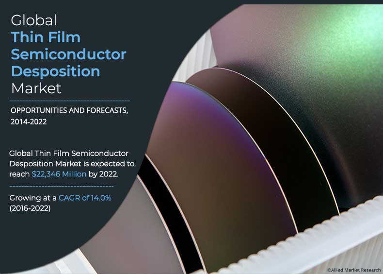
Global Thin Film Semiconductor Deposition Market is expected to garner $22 billion by 2022, registering a CAGR of 14% during the forecast period 2016 - 2022. Thin film semiconductors are the foils fabricated from artificial semiconductor materials with thickness ranging from nanometers to few hundred millimeters.
The demand for thin film semiconductors has increased in the recent years due to their advantages such as higher efficiency, lightweight, less space consumption, and flexibility in shape as compared to conventional silicon (c-Si). They are widely used in various applications such as solar panels, DRAMs, microprocessors, and wearable technologies among others.
The market is largely driven by the increasing demand of thin film solar panel and flexible electronics such as flexible display & batteries. Moreover, need for miniaturization of circuit had supplemented the growth of TFS deposition market. However, restraints associated with the TFS deposition market is huge initial investment required for setting up new manufacturing facility for TFS and increasing cost of raw materials. Moreover, growing demand of sensors in smartphone industry, and increasing application of solar systems in transportation facilities, household equipment and aircrafts are expected to create numerous opportunities for the growth of TFS deposition market in the coming years.
The demand of thin film semiconductors is expected to increase in coming years due to heavy investments on the technologies related to it. For instance, Taiwan Semiconductor Manufacturing Company Limited (TSMC), a leading wafer manufacturing company is expected to invest $3 billion to build a wafer fabrication facility in China. With the increase in demand of equipment incorporating thin film semiconductors, there will be a hike in demand of thin film semiconductors which is expected to drive the global thin film semiconductor deposition market.
Segment review
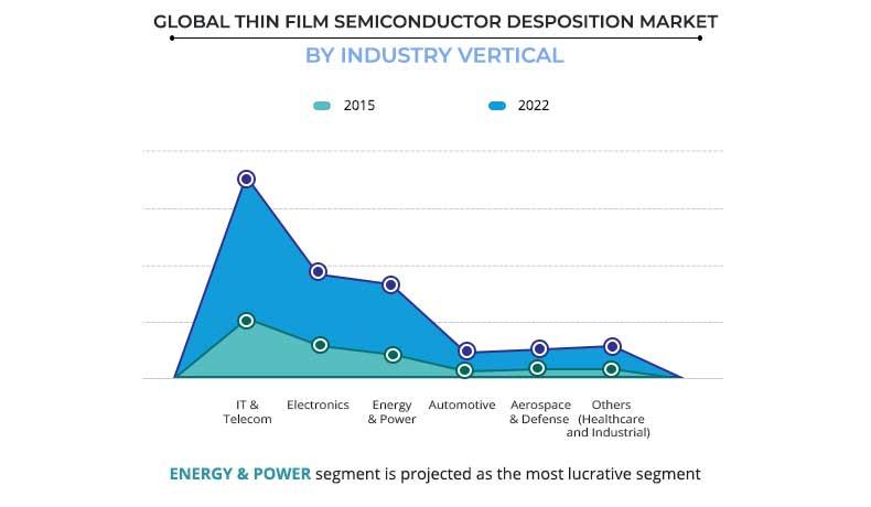
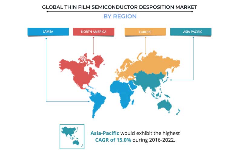
The thin film semiconductor deposition market is segmented based on type of deposition technology, industry vertical, and geography. Based on deposition technology, the market is segmented into chemical vapor deposition (CVD), physical vapor deposition (PVD), and others (epitaxy, and electro hydrodynamic deposition). Furthermore, industry vertical segment is divided into IT & telecom, electronics, energy & power, automotive, aerospace & defense, and others (healthcare and industrial). The market is analyzed on the basis of four regions, namely, North America, Europe, Asia-Pacific, and LAMEA.
Global Thin Film Semiconductor Deposition Market Scenario
Thin film semiconductors are thin foils forged of semiconductor materials with thickness in the range of nanometers to few hundred millimeters. Higher efficiency, light weight, less space requirements and flexibility in shape gives these films an edge over conventional silicon and thus these films are emerging as an apt replacement of C-Si. Major factors propelling the demand of thin film semiconductor deposition market are the extensively extending applications in rapidly growing technologies such as solar photovoltaic panels, DRAMs, microprocessors, flexible OLED displays, AMOLED displays and MEMS among others. In addition, impending need of circuit miniaturization, high investment by various governments in solar power plants and technological developments in organic LED displays also fuel up growth in the thin film semiconductor deposition market.
Top Investment pockets
The graph drawn below represents the potential of various types of deposition technology that are used to manufacture TFS. Currently, CVD technology leads the global thin film semiconductor deposition market in terms of global revenue, followed by PVD and others.
Technological superiority of thin film over conventional silicon
Conventional silicon accounts for over half of the share in the overall semiconductor market as it is the oldest material, has low price, and provides considerably high efficiency. However, after recent lab test, results of increased efficiency, the thin film materials have proved out be an apt replacement owing to their exclusive qualities such as flexible structure, less space requirement, and lightweight. These exclusive properties have escalated the growth in the global TFS deposition market. Furthermore, impending need of circuit miniaturization and low power consumption are two major factors, which drive the demand of thin film semiconductors. The impact of these two factors is expected to intensify, as the global is moving towards slim phones and displays, which require less power for their operation. Thus, the demand in thin film semiconductors is expected to boost during the forecast period.
| Properties | Thin film | Conventional silicon |
|---|---|---|
| Space consumption | Less space required for mounting hence helps in circuit miniaturization | More space required therefore, makes the whole system bulky |
| Weight | Extremely light in weight | More weight hence makes the circuit heavy |
| Flexibility | Flexible in design therefore finds extensive use in flexible and wearable devices | Sturdy and non-flexible design |
| Efficiency | Provides improved efficiency | Consumes more power and hence less efficient |
High demand due to emerging applications such as DRAM, flexible OLED displays and AMOLED displays
One of the major reasons driving the need of thin film semiconductors is the emergence of various technologies, which use them as their major application. These rapidly growing technologies include DRAMs, computer processors, flexible OLED displays, and active matrix OLED displays. These technologies are used in smartphones, TV, and other personal electronic equipment, which have a constantly increasing user base across the globe. For instance, the number of smartphone users is expected to increase from 1.5 billion to 2.5 billion from the year 2014 to 2019, which in turn is anticipated to make the impact of this factor even intense.
Key Benefits
- Comprehensive analysis of the current and future trends in the global thin film semiconductor deposition market has been provided in this report.
- The report provides a competitive scenario of the thin film semiconductor deposition market along with the growth trends, structure, driving factors, scope, opportunities, and challenges.
- The report includes a comprehensive analysis of the market segments to provide insights on the market dynamics.
- Porters Five Forces analysis highlights the potential of buyers and suppliers as well as provides insights on the competitive structure of the market to devise effective growth strategies and facilitate better decision-making.
- Value chain analysis provides key inputs on the role of stakeholders involved at various stages of the value chain.
Thin Film Semiconductor Deposition Market Report Highlights
| Aspects | Details |
| By Deposition Technology |
|
| By Industry Vertical |
|
| By Geography |
|
| Key Market Players | Ihi Hauzer Techno Coating B.V, Tokyo Electron Limited, Aixtron Se, Shin-Etsu Chemical Co., Ltd, CVD Equipment Corporation, Lam Research Corporation, Sumco Corporation, Hitachi Kokusai Electric INC, Applied Materials, Inc., Oerlikon Balzers |
Loading Table Of Content...

