
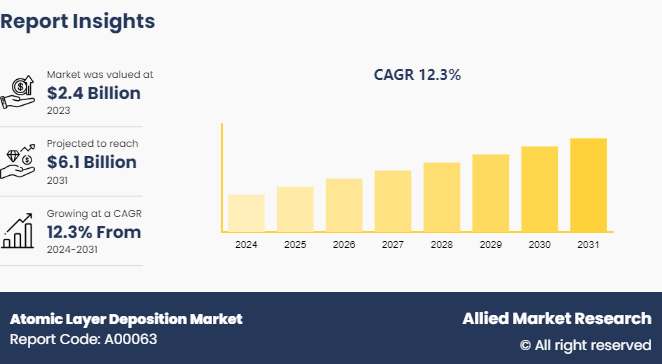
The global atomic layer deposition market was valued at $2.4 billion in 2023, and is projected to reach $6.1 Billion by 2031, growing at a CAGR of 12.3% from 2024 to 2031.
Market Introduction and Definition
Atomic layer deposition (ALD) is a precise and advanced thin-film deposition technique used in nanotechnology and materials science. It involves depositing thin films of materials onto substrates in a layer-by-layer fashion with atomic-level control and precision. ALD relies on sequential, self-limiting surface reactions between gaseous precursor molecules and a substrate surface to achieve ultra-thin and conformal coatings.
One of the key properties of ALD is its ability to deposit uniform and pinhole-free films with thicknesses ranging from a few nanometers to tens of nanometers. This uniformity and conformity make ALD suitable for coating complex three-dimensional structures and nanostructures without causing significant material loss or altering the substrate's properties. Moreover, ALD offers excellent thickness control, allowing precise tuning of film thicknesses at the atomic scale. This capability is critical for applications requiring precise thickness control, such as in semiconductor manufacturing, catalysis, energy storage devices, and advanced optics. ALD films are known for their high density, excellent adhesion, and uniformity across large-area substrates, making them indispensable in the development of next-generation materials and devices where precise film properties are paramount.
Key Takeaways
- The atomic layer deposition market report study covers 20 countries. The research includes a segment analysis of each country in terms of value for the projected period.
- More than 1, 500 product literatures, industry releases, annual reports, and other such documents of major atomic layer deposition industry participants along with authentic industry journals, trade associations' releases, and government websites have been reviewed for generating high-value industry insights.
- The study integrated high-quality data, professional opinions and analysis, and critical independent perspectives. The research approach is intended to provide a balanced view of global markets and to assist stakeholders in making educated decisions to achieve their most ambitious growth objectives.
Key market dynamics
The growth in the medical and healthcare sector is significantly driving the growth of atomic layer deposition market shares. ALD technology is increasingly being adopted in the development of advanced medical devices and implants due to its ability to produce ultra-thin, uniform, and high-quality coatings. These coatings enhance the biocompatibility, durability, and performance of medical devices, making them more reliable for long-term use in the human body. Additionally, ALD is used in the production of precise and miniaturized components for medical diagnostics and imaging equipment, contributing to improved accuracy and effectiveness in medical procedures.
The rising demand for innovative medical treatments and devices, coupled with the continuous advancements in healthcare technology, is fostering the need for high-performance materials that ALD can provide. As healthcare providers strive to improve patient outcomes and develop cutting-edge medical solutions, the role of ALD in ensuring the quality and functionality of these technologies becomes increasingly crucial, thereby propelling the market growth in this sector. High capital and operational costs pose significant restraints to the growth of the Atomic Layer Deposition (ALD) market. The initial investment required for ALD equipment is substantial, encompassing advanced deposition tools and specialized infrastructure. This financial burden is particularly challenging for small and medium-sized enterprises (SMEs) aiming to adopt ALD technology. Beyond the initial setup, operational expenses remain high due to the need for regular maintenance, energy consumption, and the use of costly precursor materials. These ongoing costs can deter companies from fully integrating ALD into their manufacturing processes. Additionally, the requirement for highly skilled personnel to manage and optimize the ALD process further adds to the operational costs. This combination of high initial and ongoing expenses can limit the widespread adoption of ALD, despite its potential to enhance product performance in industries such as electronics, semiconductors, and coatings. Therefore, addressing these cost-related challenges is crucial for the broader implementation and atomic layer deposition market growth
The growth in the energy sector presents a significant opportunity for the atomic layer deposition market size. As the demand for renewable energy sources, such as solar and wind power, increases, the need for high-efficiency energy storage and conversion devices becomes more critical. ALD plays a crucial role in the development of advanced batteries and supercapacitors by providing ultra-thin, uniform coatings that enhance the performance and longevity of these devices. Additionally, ALD is instrumental in manufacturing high-efficiency photovoltaic cells, where precise control over thin film deposition improves light absorption and overall efficiency. The increasing focus on energy efficiency and sustainability drives innovation in materials and technologies, where ALD's ability to create conformal coatings at the atomic level is highly valued. This surge in demand from the energy sector is expected to propel the growth of the ALD market, making it a vital technology in the pursuit of cleaner and more efficient energy solutions.
Patent Analysis of Global Atomic Layer Deposition Market
Based on the patent data provided, the Atomic Layer Deposition (ALD) market exhibits significant activity and concentration in key regions globally. The U.S. leads with 30.50% of the patents, underscoring its robust research and development landscape in ALD technology. China follows closely with 24.74%, highlighting its rapid advancements and investment in semiconductor and electronics industries. South Korea and Japan also demonstrate substantial presence at 16.68% and 7.94% respectively, reflecting their strong positions in semiconductor manufacturing and nanotechnology applications. These figures indicate a competitive and innovative ALD market, driven by technological advancements and regional expertise in materials science and electronics manufacturing.

Market Segmentation
The atomic layer deposition market is segmented into product, application and region. By product, the market is classified into thermal, metal, plasma-enhanced, and others. By application, the market is divided into semiconductors and electronics, healthcare and biomedical, automotive, and others. Region-wise the market is analyzed across North America, Europe, Asia-Pacific, and LAMEA.
Competitive Landscape
The major players operating in the atomic layer deposition market include Forge Nano Inc., Beneq Group, Oxford Instruments, Applied Materials, Inc., LAM RESEARCH CORPORATION, ASM International N.V., Kurt J. Lesker Company, Veeco Instruments Inc., Entegris Inc, and Picosun Oy.
Recent Key Strategies and Developments
- In February 2024, Applied Materials has unveiled a collaboration with semiconductor industry suppliers to expedite the establishment of a sustainable semiconductor ecosystem in India. The initiative aims to accelerate the development of subsystems and components for semiconductor equipment by bringing together engineers, domestic and international suppliers, as well as research and academic institutions at the Engineering Centre.
- In February 2024, ASMS represents the leading-edge technique in the market, driven by the increasing demand for advanced chips and memory due to the growth of generative AI. This technology focuses on sub-3 nm nodes where Atomic Layer Deposition (ALD) excels. ALD is crucial for producing high-end chips and contributes significantly to half of ASMS's equipment revenues. Recently, the company has made notable strides in Silicon Epitaxy and has entered the rapidly expanding Silicon Carbide sector, enhancing its market presence.
- In November 2023, Oxford Instruments Plasma Technology has announced substantial orders for plasma atomic layer deposition (ALD) and atomic layer etch (ALE) systems from leading Japanese foundries. These systems are specifically intended for the production of GaN HEMT devices, crucial for the rapidly expanding markets of GaN power electronics and radio frequency applications. Key focuses include consumer fast-charging and datacenter applications in the power electronics sector, while 5G/6G communication applications dominate the radio frequency market.
- In September 2023, KY Water Technology unveiled its plan to offer customers a new semiconductor processing tool, the Applied Picosun MorpherTM for atomic layer deposition (ALD) . This tool enables the uniform deposition of thin layers across silicon wafers, essential for various devices including sensors and emerging memory technologies.
- In July 2021, Picosun Group expanded its global sales and service partner network through a collaboration with Hermes-Epitek Corporation Ptv. Based in Taiwan, Hermes-Epitek Corporation is renowned as one of the largest distributors of high-tech equipment globally.
- In June 2021, The Kurt J. Lesker Company developed precise atomic layer deposition (ALD) techniques for applying titanium (IV) oxide (TiO2) thin films onto Polymethyl Methacrylate (PMMA) . These processes demonstrate outstanding surface quality and mechanical characteristics, making them suitable for diverse applications in engineering, medical, and biomedical fields.
- In March 2021, Canon and Tokyo Electron have teamed up to participate in Japan's advanced chip manufacturing initiative. Tokyo Electron, a leading supplier of chip manufacturing equipment, and Canon, renowned for its semiconductor lithography equipment, along with Screen Semiconductor Solutions, which specializes in wafer-coating and cleaning equipment, are collaborating on this strategic endeavor.
Regional Market Outlook
Asia-Pacific is experiencing robust economic growth. The expanding electronic industry in Asia-Pacific is poised to drive significant growth in the atomic layer deposition market analysis across the region. There is an increasing demand for advanced thin film deposition technologies like ALD as countries like China, South Korea, and Taiwan continue to lead in electronics manufacturing. These technologies are crucial for enhancing semiconductor performance, improving energy efficiency, and enabling the production of miniaturized electronic components. This trend is expected to fuel the adoption of ALD solutions, supporting further technological advancements and atomic layer deposition market forecast in Asia-Pacific.
- Asia-Pacific remains the foremost region driving the expansion of the electronics industry, serving as a central hub for OEMs. Emerging economies such as Vietnam have made substantial investments in this sector, fostering robust competition among regional countries. Meanwhile, established hubs like Taiwan and China maintain strong commitments to research and development, positioning themselves at the forefront of innovative advancements that propel market expansion. This dynamic environment underscores Asia-Pacific's pivotal role in shaping the global landscape of the electronics industry.
- Atomic Layer Deposition (ALD) is widely used in solar cells and devices for conformal coatings. The market is expected to grow during the forecast period, driven by the increasing demand for solar devices and the expansion of the solar industry across various countries in the Asia-Pacific region. Furthermore, governments in the Asia-Pacific region are consistently investing in initiatives to boost their solar industries, thereby fueling the demand for ALD solutions.
- Asia-Pacific hosts some of the largest automobile manufacturers globally, including Honda, Toyota, Mitsubishi, Nissan, Hyundai, TATA Motors, and Maruti. Countries like China, India, Japan, and South Korea are prominent hubs in the Asian automotive sector. Besides these original equipment manufacturers (OEMs) , numerous suppliers of parts and automobile accessories also utilize ALD units and equipment for their manufacturing needs.
- Atomic layer deposition (ALD) is a crucial method in semiconductor device manufacturing, involving a gas-phase chemical process for thin-film deposition. Key industry players in this region are heavily focusing on research and development initiatives aimed at enhancing efficiency and driving rapid market expansion globally.
- Therefore, Asia-Pacific is projected to emerge as a dominant force in the atomic layer deposition market overview throughout the forecast period.
Industry Trends:
- Atomic Layer Deposition (ALD) technology is driven primarily by demand from the semiconductor and electronics industries. The semiconductor sector directly influences its development, while any expansion in the electronics industry also contributes to its advancement. Consequently, there is growing demand for ALD equipment.
- Following global fab capacity expansions in response to the chip shortage, ALD players are poised to capitalize on new growth opportunities. Recently, 300mm ALD platforms have been enhanced to meet the requirements of More-than-Moore (MtM) devices such as MEMS, sensors, power and RF devices, and photonics. Previously, 200mm ALD platforms were sufficient for market needs, but now with increased wafer production volumes, ALD solutions are expected to expand into the MtM devices market.
- ALD gained prominence in the semiconductor industry for depositing high-permittivity oxide materials, like replacing thermally grown SiO2 with ALD-formed HfO2 as gate dielectric materials in metal oxide semiconductor field-effect transistors (MOSFETs) . The number of applications requiring ALD has significantly grown in recent years.
- The electronics sector experiences cyclical fluctuations. The short- to medium-term outlook for the industry is positive, driven by significant growth in mobile subscriptions, mobile broadband, and unique mobile users forecasted by the Ericsson Mobility Report for 2024. This growth is expected to accelerate the adoption and development of ALD technology.
- Furthermore, the increase in demand for semiconductor integrated circuits (ICs) in consumer electronics and microelectronics is anticipated to boost semiconductor device manufacturers' production capabilities, thereby driving demand for ALD equipment. ALD's ability to deposit highly conformal films like SiO2, SiNx, and SiC at low temperatures is crucial for next-generation semiconductor device production, replacing traditional methods like chemical vapor deposition.
- Moreover, ALD enhances the performance and reliability of RF and power electronics under extreme environmental conditions, further supporting its technological advancement.
Key Sources Referred
- Ericsson Mobility Report
- IEA
- Our World In Data
- India Ministry of Coal statistics
- The Ministry of Power
- The National Institution for Transforming India (NITI Aayog)
- USDA
Key Benefits for Stakeholders
- This report provides a quantitative analysis of the atomic layer deposition market segments, current trends, estimations, and dynamics of the market analysis from 2023 to 2031 to identify the prevailing market opportunities.
- Market research is offered along with information related to key drivers, restraints, and opportunities.
- Porter's five forces analysis highlights the potency of buyers and suppliers to enable stakeholders to make profit-oriented business decisions and strengthen their supplier-buyer network.
- In-depth analysis of the atomic layer deposition market segmentation assists in determining the prevailing market opportunities.
- Major countries in each region are mapped according to their revenue contribution to the global atomic layer deposition market Statistics.
- Market player positioning facilitates benchmarking and provides a clear understanding of the present position of the market players.
- The report includes the analysis of the regional as well as global atomic layer deposition market trends, key players, market segments, application areas, and market growth strategies.
Atomic Layer Deposition Market Report Highlights
| Aspects | Details |
| Market Size By 2031 | USD 6.1 Billion |
| Growth Rate | CAGR of 12.3% |
| Forecast period | 2024 - 2031 |
| Report Pages | 280 |
| By Product |
|
| By Application |
|
| By Region |
|
| Key Market Players | Forge Nano Inc., Oxford Instruments, ASM International N.V., Kurt J. Lesker Company, Entegris, Inc., Applied Materials, Inc., Beneq Group, Veeco Instruments Inc., Picosun Oy., LAM RESEARCH CORPORATION |
Loading Table Of Content...

