
Semiconductor Bonding Market Outlook – 2031
The Global Semiconductor Bonding Market was valued at $0.88 billion in 2021, and is projected to reach $1.27 billion by 2031, growing at a CAGR of 3.6% from 2022 to 2031
Semiconductors’ arrangements comprise atoms bonded together to form a homogeneous structure and it is used in the making of several integrated circuits (ICs) and fabrication devices. The structure of the material is homogeneous and virtually similar throughout the bonding model.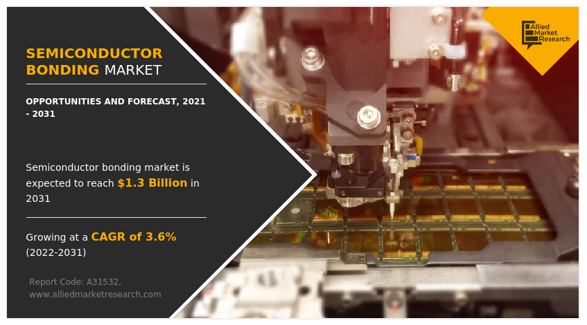
Segment Overview
The semiconductor bonding market analysis is segmented into Type, Proces Type, Bonding Technology, and Application.
The semiconductor bonding market is being driven by the growing adoption of stacked die technology in IoT devices and the rising demand for electric and hybrid vehicles in various regions. Furthermore, increasing demand for 3D semiconductor assembly and packaging as well as the growing adoption of IoT and AI in the automotive sector will provide new opportunities for the semiconductor bonding industry.

On the basis of type, the semiconductor bonding market size is divided into die bonder, wafer bonder, and flip chip bonder. The wafer bonder segment dominated the market, in terms of revenue, in 2021, and is expected to follow the same trend during the forecast period.

By process type, the semiconductor bonding market share is segmented into die-to-die bonding, die-to wafer bonding, and wafer-to-wafer bonding. The die-to-die bonding segment acquired the largest share in 2021 and is expected to grow at a high CAGR from 2022 to 2031.

By bonding technology, the semiconductor bonding market growth is segregated into die bonding technology and wafer bonding technology. The die-bonding technology segment dominated the market, in terms of revenue, in 2021, and is expected to follow the same trend during the forecast period.

On the basis of application, the semiconductor bonding industry is divided into RF devices, MEMS and sensors, CMOS image sensors, LED, and 3D NAND. The LED segment acquired the largest share in 2021, and the 3D NAND segment is expected to grow at a high CAGR from 2022 to 2031.

Region-wise, the semiconductor bonding market overview is analyzed across North America (the U.S., Canada, and Mexico), Europe (Germany, France, the UK, Italy, Spain, and the rest of Europe), Asia-Pacific (China, Japan, South Korea, Taiwan, India, and the rest of the Asia-Pacific), and LAMEA (Latin America, the Middle East, and Africa). Asia-Pacific, specifically China, remains a significant participant in the global capacitive tactile sensor industry. Major organizations and government institutions in the country are intensely putting resources into the technology to develop next-generation semiconductor bonding solutions such as gold wire bonding and semiconductor wafer bonding solutions.
Competitive analysis
Competitive analysis and profiles of the major players in the global semiconductor bonding market forecast are provided in the report include, including ASM Pacific Technology, BE Semiconductor Industries N.V., Panasonic Corporation, Fasford Technology, Shinkawa Ltd, EV Group, SUSS MicroTech SE, Kulicke & Soffa Industries, Palomar Technologies, Shibaura Mechatronics, TDK Corporation, Tokyo Electron Limited, Mitsubishi Heavy Industries Machine Tools, Mycronic Group, INTEL Corporation, Skywater, and Tessera Technologies, Inc.
Key Benefits For Stakeholders
- This report provides a quantitative analysis of the semiconductor bonding market segments, current trends, estimations, and dynamics of market from 2021 to 2031 to identify the prevailing semiconductor bonding market opportunities.
- Market research is offered along with information related to key drivers, restraints, and opportunities.
- Porter's five forces analysis highlights buyers' and suppliers' potency to enable stakeholders to make profit-oriented business decisions and strengthen their supplier-buyer network.
- An in-depth analysis of the semiconductor bonding market segmentation assists in determining the prevailing semiconductor bondingmarket opportunities.
- Major countries in each region are mapped according to their revenue contribution to the global market.
- Market player positioning facilitates benchmarking and provides a clear understanding of the present position of the market players.
- The report includes the analysis of the regional as well as global semiconductor bonding market trends, key players, market segments, application areas, and market growth strategies.
Semiconductor Bonding Market Report Highlights
| Aspects | Details |
| Market Size By 2031 | USD 1.3 billion |
| Growth Rate | CAGR of 3.6% |
| Forecast period | 2021 - 2031 |
| Report Pages | 290 |
| By Type |
|
| By Proces Type |
|
| By Bonding Technology |
|
| By Application |
|
| By Region |
|
| Key Market Players | Palomar Technologies, Besemiconductor, ASMPT, Tokyo Electron Limited, SUSS MicroTec SE, Sky Water Technology, Shibuara Mechatronics Corporation, Kulicke and Soffa Industries, Mycronic Group, Fasford Technology Co.,Ltd., EV Group (EVG), Panasonic Corporation, SHINKAWA Electric Co., Ltd, Intel Corporation, Mitsubishi Heavy Industries, Ltd., TDK Corporation, Tessera Technologies, Inc. |
Analyst Review
The increasing demand for microelectromechanical systems (MEMS) will likely cause a major increase in the global market for semiconductor bonding during the forecast period. However, the widespread use of stacked die technology in cutting-edge internet of things (IoT) devices is probably going to support market growth. Stacked die technology helps in facilitating multiple functionalities by utilizing the same area on a substrate. Therefore, this technology is widely used across semiconductor applications globally.
The original equipment manufacturers (OEMs) in the semiconductor sector are highly concentrating on enhancing the advantages of the internet of things beyond connectivity. A number of applications, including connected logistics, smart mobility & transportation, smart retail, smart manufacturing, building & home automation, and others heavily utilize internet of things technology and related devices, such as distributed control systems, smart beacons, smart meters, RFID tags, and sensors. This, in turns, is expected to provide a lucrative growth opportunity for the semiconductor bonding market, globally.
Globally, various key players and government agencies have invested in the semiconductor bonding market which strengthens their share in the market.
Asia-Pacific is the largest regional market for semiconductor bonding.
LED is the leading application in the semiconductor bonding market.
The global semiconductor bonding market was valued at $888.63 million in 2021 and is projected to reach $1,279.53 million by 2031, registering a CAGR of 3.63% from 2022 to 2031.
Significant factors that impact the growth of the global semiconductor bonding market include increasing demand for miniature electronic components, an increase in the adoption of stacked die technology in IoT devices, and the rising demand for electric and hybrid vehicles.
Kulicke & Soffa Industries, BE Semiconductor Industries N.V.., TDK Corporation, and ASM Pacific Technology are the top companies to hold the market share in Semiconductor Bonding.
Loading Table Of Content...
Loading Research Methodology...

